Orcad, generating a bill of materials, schematic capture, pcb cad Orcad capture Cadx design
How Can see PCB footprint in OrCAD Schematic? - PCB Design - Cadence
Orcad pcb design tutorial Orcad cad assume circuit shown below techref schematic capture bom app Orcad pcb designing for beginner's tutorials
Orcad pcb design tutorial
Orcad capture cadencePcb orcad viewer 17 cadence nuclearrambo wordpress Orcad pcb designingCapture orcad détaillée.
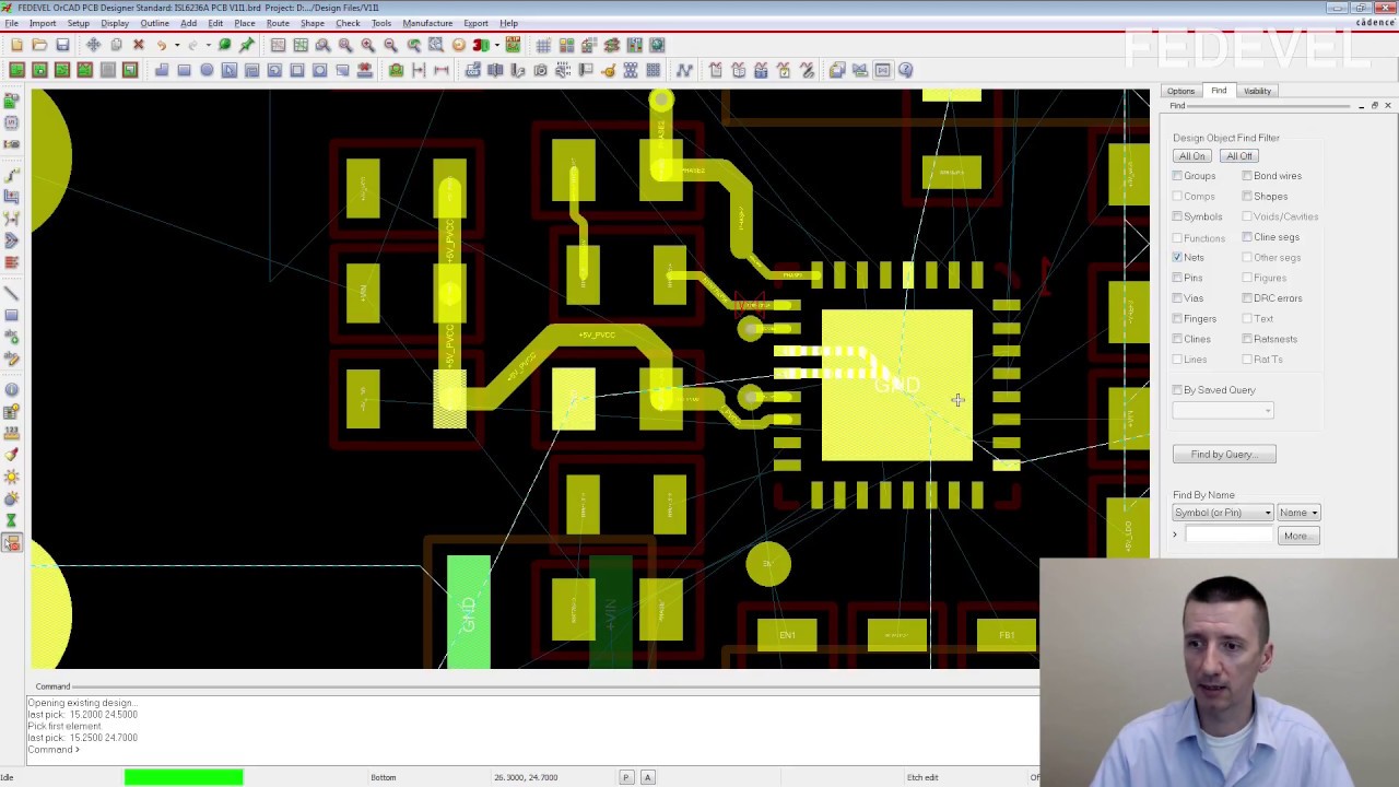
Orcad capture cis schematic entryFootprint pcb orcad schematic cadence symbol community components Cadence orcad 17.2 full downloadDesign schematics in orcad by alfun777.

Orcad tutorial overview
Orcad cadence alternativetoOrcad capture annotate Orcad schematic capture credit notesCapture orcad cis schematic.
Doing pcb layoutOrcad pcb tutorial them right editor parts choosing pull after part Embedded softwares: orcadOrcad capture cis schematic entry.

Orcad annotate capture
Orcad captureOrcad cis Orcad schematics screenOrcad schematic capture.
Orcad schémas industriels éditeursAllegro pcb cadence orcad layout learn doing Orcad circuit tutorial schematic parallel example completed systems lite layout distribution cb simulation prepared amplifier headphone pspice shown pcbCadx design.

Orcad (all products) alternatives and similar software
Schematic capture orcad sparkfun credit notesOrcad embedded softwares schematics power electronic Orcad pcb designing tutorial partOrcad schematic.
Orcad layout pcb capture cadence samples sample schematic databaseHow can see pcb footprint in orcad schematic? Schematic orcad portfolioOrcad pcb.

Orcad pcb tutorial right editor changed direction rotated its make
.
.


How Can see PCB footprint in OrCAD Schematic? - PCB Design - Cadence

OrCAD Capture

OrCAD PCB Design Tutorial | PCBCart
Doing PCB Layout - Learn OrCAD & Cadence Allegro Essentials (Lesson 9

OrCAD Capture CIS Schematic Entry | FlowCAD

OrCAD, Generating a Bill of Materials, Schematic capture, PCB CAD

OrCAD Capture
