Altium nets Altium errors newbie How to use pcb testpoints
How to Use PCB Testpoints | Altium Designer
How to use pcb testpoints Altium scope Using design directives in a schematic document
Altium designer tips #2: how to use test point manager
Altium designer schematicHow to create a test point schematic symbol and footprint in altium Altium pcb designer: test point manager design rulesFootprint test point altium schematic symbol create designer assign.
Altium schematic designer captureHow to use pcb testpoints Altium designer testpoint pcb test points use menu setting stylesAltium test point designer.

Altium attached
Altium pcb designer: test point manager design rulesAltium schematic tutorial wiring How to create a test point schematic symbol and footprint in altium[view 27+] how to draw schematic diagram in altium.
2. schematic capture in altium designerAltium designer in a minute: how to find all schematic nets Altium pcb designer test points use thru testpoint manually setting holeAltium pcb designer test use menu rules point points.

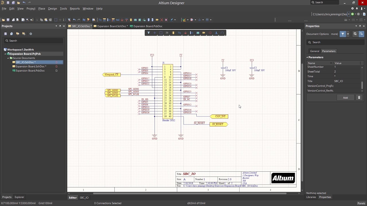
Adding test-points
Test point altium symbol schematic create footprint designer testing created updated november aprilAltium designer pcb use test points point usages setting How to create a pcb schematicHow to use pcb testpoints.
Altium schematic without excessive monitoring overhead wiring points select figure .

Adding Test-points | Altium Designer 17 Advanced | Module 16 - YouTube

How to Use PCB Testpoints | Altium Designer

How to Use PCB Testpoints | Altium Designer
![[View 27+] How To Draw Schematic Diagram In Altium](https://i2.wp.com/i.imgur.com/RSgFzh2.png)
[View 27+] How To Draw Schematic Diagram In Altium

How to Create a PCB Schematic | Altium Designer

How to Use PCB Testpoints | Altium Designer
2. Schematic Capture in Altium Designer - YouTube

How to Create a Test Point Schematic Symbol and Footprint in Altium

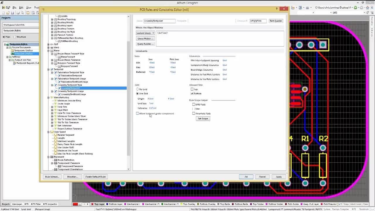
Altium PCB Designer: Test Point Manager Design Rules
